- 20th INTERNATIONAL SYMPOSIUM "NANOSTRUCTURES: PHYSICS AND TECHNOLOGY"
- Nanotech Europe 2009
- SMART SYSTEMS INTEGRATION 2009
- The 14th Canadian Semiconductor Technology Conference (CSTC-2009) and the 4th Nano & Giga Forum (NGC-2009 - Nano & Giga Challenges in Electronics, Photonics, and Renewable Energy).
- http://www.ioffe.ru/natoarw/2009/ 29 June –02 July, 2009
- Design, Test, Integration & Packaging of MEMS/MOEMS
- V МЕЖДУНАРОДНАЯ ВЫСТАВКА NTMEX 08
- 5th International Technology Transfer Days BIOMATERIAL 2009
- COMS - Commercialization of Micro and Nano Systems Conference, 31st August - 4th September 2008, Puerto Vallarta, Mexico
- ICCE - Integration and Commercialization of Micro and Nanosystems International, 3rd - 5th June 2008, Hong Kong, China
- The Fourth International Conference on "Science and Business": NanoBio and Related New and Perspective Biotechnologies Pushchino Biological Center of Russian Academy of Sciences Moscow Region, Russia, October 15 - 18, 2007.
- MicroNanoWorld
- SYMPOSIUM on Design, Test, Integration and Packaging of MEMS/MOEMS
- Micro-Nano Technologies for Aerospace Applications From Concepts to Systems.
- 20th Eurosensors Conference Anniversary
- Symposium and School on Nano
and Giga Challenges in Electronics and Photonics:
from Atoms to Materials to Devices
to System Architecture - MEMS & MST Conference
- I A R P
International Advanced Robotics Programme - 10th International Conference on the Commercialization of Micro and Nano Systems
COMS 2005 - ICMNE 2005 QI-2005
International Conference “Micro-& nanoelectronics-2005”
and International Symposium “Quantum Informatics – 2005” - Symposium on Design, Test, Integration and Packaging of MEMS / MOEMS
- International Congress of Nanotechnology 2004
- PEM-2004
Ninth International Science Conference
"Actual Problems of Solid-State Electronics and Microelectronics" - Int'l Workshop on MEMS and NANOTECHNOLOGY INTEGRATION (MNI): APPLICATIONS
- NATO
Advanced Research Workshop
Science and Technology of Semiconductor-On-Insulator structures and devices operating in a harsh environment - Symposium on Desigen, Test, Integration and Packaging of MEMS / MOEMS 2004
- European Micro and Nano systems 2004
- MANCEF - Micro and Nanotechnology Commercialization Education Foundation
- IEE Proceedings – Science, Measurement and Technology
- 10th Saint Petersburg international conference on integrated navigation systems
- 11th International Symposium «NANOSTRUCTURES: PHYSICS AND TECHNOLOGY»
- Word Microtechnologies Congress "MICRO.tec 2003"
- Nanotechnology Conference and Tradeshow "NanoTech 2003"
- International conference on microrobots, micromachines and microsystems
- Design, Test, Integration and Packaging of MEMS / MOEMS
- IV International scientific-technical conference "Electronics and information science - 2002"
Int'l Workshop on MEMS and NANOTECHNOLOGY
INTEGRATION (MNI): APPLICATIONS
10-11 May 2004 -
Hotel Eden au Lac - Montreux, Switzerland.
Invitation
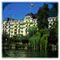
The Workshop will be held at the Hotel EDEN AU LAC
in Montreux, Switzerland
MOTIVATION
A Workshop on MEMS and Nanotechnology Integration will be held on 10-11 May 2004, under the auspices of the Aviation and Missile Research Development Engineering Center, European Research Office, US Army. The Workshop will be co-located with the Symposium on Design, Test, Integration and Packaging of MEMS/MOEMS to be held on 12-14 May 2004 in Montreux, Switzerland. Applications for MEMS devices continue to expand as the fabrication technology advances. But device requirements for system integration require a careful look at the technology issues that limit performance and lifetime or that restrict the architectural designs possible. These designs include compatibility of materials, mechanical interactions, electrical interconnection, vibration effects, thermal management, and vacuum or packing constraints. In additions, many of the device applications lend themselves to geometrical scaling extending to the NANO level, thus further challenging traditional approaches for stimulation or pick-off of signals and information. The use of optical techniques together with MEMS devices adds to the concerns of material choices and design requirements. Further advancements in the integration of MEMS and NANO devices for applications in inertial or environmental sensors, actuators, controllers, micro fluidics, RF components, and energy conversion will depend upon resolving the associated technical barriers.
OBJECTIVES
The workshop will focus on the identification of these technical barriers or issues, and then explore the possible approaches for solution. The program is arranged to provide adequate time for technical discussion stimulated by invited presentations directed toward a better understanding of the technical applications and issues of MEMS and NANO device integration. A broad range of technical expertise is expected to be represented by the workshop participants with opportunities for future technical collaborations. The results of the workshop will be collected and reported as part of a panel discussion during the Symposium on DTIP of MEMS/MOEMS (Thursday 13 May 2004).
TOPICS
The topics of special interest include:
- Alternate Materials
- Electronic Integration with MEMS Devices
- Environmental Effects
- Extension of MEMS to Nano Scale
ORGANIZING AND SCIENTIFIC COMMITTEE:
P. Ashley, AMRDEC, Redstone Arsenal, USA;
M. Marchetti, U. of Roma "La Sapienza", Italy;
P. Stevens, QinetiQ, UK;
L. Murdock, AMRDEC- European Research Office, London, UK;
M. Regi, U. of Roma "La Sapienza", Italy;
P. Ruffin, AMRDEC, Redstone Arsenal, USA;
M. Lyon, AMRDEC, Redstone Arsenal, USA;
Registrations must be sent in by April 23, 2004.
There is no registration fee for the workshop but everyone is required to register online for the Workshop and Symposium since there will be no on-site registration on the day of the workshop. To register for the workshop and the DTIP Symposium go to:
http://tima.imag.fr/conferences/dtip/DTIP2004/index.html).
MEMS and NANO Integration Workshop
PROGRAM
|
Monday, May 10, 2004
|
|
12:00-1:00
|
|
|
1:00-1:45
|
Introduction and Overview of Issues, Paul Ashley, U.S. Army
|
Session 1
Alternate Materials
Alma Wickenden, Session Chair
|
|
1:45-2:15
|
"Development of Mesoporous Oxide Films MEMS Structures"
Bruce Dunn, University of California Los Angeles, USA
|
|
2:15-2:45
|
"Advantages and Challenges of Piezoelectric MEMS/NEMS Device Technology"
Alma Wickenden, U.S. Army
|
|
2:45-3:00
|
Break
|
|
3:00-3:30
|
"MEMS Technology Based on CVD-Diamond"
Ralph Mueller, University of ULM, Germany
|
|
3:30-4:15
|
Workshop Discussion
|
|
7:00-9:00
|
Reception
|
Tuesday, May 11, 2004
Session 2
Electronic Integration of MEMS Devices
Marc Polosky, Session Chair
|
|
8:00-8:30
|
"Electrical and Optical Integration of Microsystems"
Marc Polosky and Gerard Sleefe, Sandia National Lab, USA
|
|
8:30-9:00
|
"CMOS Compatible MEMS for Monolithically Integrated Microsystems"
David King, QinetiQ, Malvern, UK
|
|
9:00-9:30
|
"Integration Approaches for Non-silicon MEMS"
Mark Allen, Georgia Tech University, USA
|
|
Special Topics on MEMS Integration
|
|
9:30-9:45
|
"Recent developments in membrane supported millimeter wave circuits at IMT Bucharest"
A Muller, D Neculoiu and D.Dascalu IMT Bucharest, Romania
|
|
9:45-10:00
|
"Why Do We Need a Surface Micromachining Technology with an On-Chip Integrated CMOS Electronics?"
Andrzej Napieralski, Krzysztof Szaniawski, Technical University of Lodz, Poland
|
|
10:00-10:45
|
Workshop Discussion/Break
|
Session 3
Environmental Effects of MEMS Devices
Fred Sexton , Session Chair
|
|
10:45-11:15
|
"What Will It Take to Have Reliable Microsystems?"
Fred Sexton, Sandia National Lab, USA
|
|
11:15-11:45
|
"The Impact of Harsh Operational Environments on MEMS Design, Packaging, and Performance"
Mike Kranz, Morgan Research Corp., USA
|
|
11:45-12:45
|
Lunch
|
|
12:45-1:15
|
TBD
|
|
1:15-1:45
|
Workshop Discussion
|
Session 4
Extension to NANO Scale
Mario Marchetti/Marco Regi, Session Chairs
|
|
1:45-2:15
|
"Transition and Utilization of Nanotechnology for Energetic Applications"
Mike Lyon and Richard Hatcher, U.S Army
|
|
2:15-2:45
|
"Design and Charactererization of Anisogrid Lattice Structures with Carbon Nanotubes"
Mario Marchetti, Marco Regi, University of Rome, F.Mancia, Centro Sveluppo Materiali (C.S.M.) Pomerzia of Rome, Italy
|
|
2:45-3:15
|
"From Micro-Mechanics to Molecular Scale Mechanics"
Panos Datskos, Oak Ridge National Labs, USA
|
|
3:15-3:30
|
Break
|
|
Special Topics on NANO Technology
|
|
3:30-3:45
|
"Boron and Carbon Doped Self-Assembling Biological Superstructures for Molecular Scale Sensory Elements"
Kervalishvili Paata, Mrevlishvili George, Tbilisi State University, Georgia
|
|
3:45-4:00
|
"Characterization of Nano-Aluminized High-Energy Materials (HEM)"
L. Galfetti, F. Severini, G. Colombo, L.T. DeLuca, SP Lab, Politecnico di Milano,
Italy, L. Meda, Polimeri Europa, Italy A. Vorozhtsov, Institute for Problems of Chemical & Energetic
Technologies, Russia, V. Sedoi, Institute of High Current Electronics, Russia, V. Babuk, BSTU, Russia,
and B.N. Kondrikov, Mendeleev University, Russia
|
|
4:00-4:15
|
"Nanostructures, as New Object of Study of the Natural World Properties, Condition of Application and Obtaining"
Valery A. Babuk, Baltic State Technical University, Russia
|
|
4:15-4:30
|
"Production of Nanosized Powders and Coatings by the Exploding Wire Method"
M. Osmonoliev, V. Sedoi, Institute of High Current Electronics, Russia, A. Vosmerikov, Institute of Petroleum Chemistry, Russia, N. Zamyatin, Institute of High Current Electronics, Russia
|
|
4:30-4:45
|
"Advanced Technologies of Controlled Manufacturing and the Use of Nanometals in High-Energy Materials (HEM) Formulation"
M. Lerner, Advanced Powder Technology Ltd., Russia, G. Pavlovets, V. Meleshko, Peter
Research Center, Russia, A. Vorozhtsov, Institute for Problems of Chem. & Energ. Techn., SB RAS, Russia, V. Arkhipov, Tomsk State University, Russia, and L. DeLuca, Politecnico di Milano, Italy
|
|
4:45-5:15
|
"Synthesis of Small-Scale Boran-Rich NANO-Size Particles"
Vladislav G. Slutsky, Sergei A. Tsyganov and Eugeny S. Severin, Russian of Sciences, Russia
|
|
5:15-5:30
|
Workshop Discussion
|
|
5:30-5:45
|
Workshop Wrap-up and Conclusions
|
|